
 EN
EN

Direct answer: Zhengna Technology supplies made-to-drawing stamped electrical terminals and battery contacts for PCB conduction, battery charging and discharging interfaces, and switch or button contacts. Material, temper, thickness, plating zones, burr direction and inspection evidence are agreed against the released drawing before production.
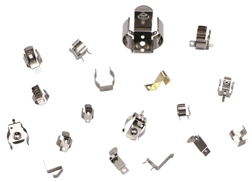
A contact drawing should separate substrate, temper and finish before tooling is released. The photograph on this page shows representative contact geometries. It does not identify the substrate, temper, plating stack, electrical rating or inspection result of every pictured part.
Start with the electrical and mechanical job
A buyer should not select a contact alloy from colour or a generic catalogue label. First define whether the part is a fixed conductive tab, a spring contact arm, a solder terminal, a grounding finger or a repeated-mating interface. That decision changes the balance among conductivity, spring recovery, fatigue resistance, forming strain, finish compatibility and cost.
For the supplied product family, typical strip thickness is 0.2-2.0 mm. The final thickness is not a current-rating claim: it must be checked with the interface geometry, allowable temperature rise, contact area, mating force and the responsible electrical design.
Material and temper options
| Material family | Typical grades and conditions | Best-fit buyer use | Important boundary |
|---|---|---|---|
| ETP copper | C11000 / C1100 / T2; commonly half hard or H04, with O temper only where a suitable deep-draw route is confirmed | Fixed conductive tabs, PCB grounding tabs, bus bridges and battery welding tabs without a spring-arm requirement | About 100% IACS conductivity does not provide the recovery expected from a spring contact arm. |
| Phosphor bronze | C5191 / C51000 / QSn6.5-0.1 in half hard, H or EH; C5210 / C52100 / QSn8-0.3 in H, EH or SH where higher spring force is required | Board-to-board contact arms, battery spring contacts, SIM contacts, button contacts and relay contact springs | C5191-family conductivity is typically about 13-18% IACS. Fatigue, force and insertion-cycle requirements still need project validation. |
| Brass | C2680 / C26000 / H65 in half hard, H or EH; C2720 or C2801 only after drawing review | Cost-sensitive battery-holder contacts, solder terminals, shielding springs and enclosure contacts | Typical conductivity is about 27-28% IACS. Brass is not automatically the best choice for a high-cycle spring arm. |
| Higher-performance copper alloys | C17200 / QBe2, C7025 / Cu-Ni-Si, C19400 or C14415, subject to material and compliance review | Projects that combine higher spring strength, fatigue, temperature or conductivity demands | C7025-family conductivity is typically about 35-45% IACS; C19400/C14415 may cover about 55-95% IACS. Exact properties depend on grade, temper and supplier records. |
| SUS301 stainless steel | Quarter hard through H where the contact design permits | Shielding springs or grounding fingers when bulk conductivity is not the primary selection driver | Do not describe SUS301 as a copper contact substrate. Electrical function depends on the confirmed geometry, mating interface and finish. |
Plating must match the interface
Tin plating in a typical 1-5 micrometre range is a cost-effective option for solderable interfaces, including suitable wave-soldering projects. A typical 2-3 micrometre nickel layer with a thin, drawing-defined gold finish can be reviewed for lower-contact-resistance or high-frequency interfaces.
The drawing should identify which faces are functional contact zones, solder zones, masked zones and cosmetic zones. It should also state the plating thickness, base layer, local or overall application, adhesion and thickness test requirements, and any soldering or mating validation owned by the project. A finish name alone does not prove solderability, contact resistance, corrosion life or signal performance.
Stamping, forming and burr control
The manufacturing review covers strip layout, grain direction where relevant, blanking and piercing, bend radii, formed height, contact-arm geometry, burr direction and the relationship between datum features and the mating interface. Tooling and process route depend on the released geometry and volume; the page does not promise one universal die type for every contact.
Typical geometric tolerances for this product family may fall within ±0.02-0.05 mm, while a typical burr-height requirement may be ≤0.03 mm. Those values are capability ranges for drawing review, not automatic acceptance limits for every feature. The drawing must identify critical-to-function dimensions, measurement datums and the surfaces where burr direction matters.
Inspection evidence for an OEM order
Critical profile, position, formed height and selected geometric features can be checked with 2D vision measurement or a coordinate measuring machine. The inspection plan should name the equipment, feature, frequency, sample size and acceptance rule. Visual appearance or equipment ownership is not a lot-release result.
- Confirm material grade, temper and thickness against the released specification.
- Identify critical dimensions, datum logic and mating-interface features.
- Define burr direction and maximum height on functional edges.
- State plating zones, layer sequence, thickness and the required evidence.
- Agree the first-piece, in-process, sampling or final-inspection frequency for the order.
MOQ, lead time and packaging
A typical standard custom order starts at 1,000 pieces, with a typical lead time of 10-15 days after technical and commercial confirmation. The confirmed schedule depends on tooling status, material availability, finish route, inspection scope and order quantity. Standard packaging uses antistatic inner bags and outer cartons unless the drawing or handling risk requires a separately agreed pack.
RFQ checklist
For a controlled quotation, send:
- 2D drawing and, when useful, a 3D model with revision level;
- material grade, temper and strip thickness;
- plating stack, thickness, zones and masked areas;
- annual and order quantity, project stage and required delivery date;
- critical dimensions, burr direction and acceptance limits;
- mating interface, required spring action and responsible electrical-performance criteria;
- soldering process, inspection evidence and packaging requirements.
Review the broader PCB hardware stamping capability, the custom stamping service, or send the drawing to Zhengna Technology for an RFQ review.
Frequently asked questions
Which material is suitable for a stamped battery contact?
ETP copper fits fixed conductive tabs; phosphor bronze fits many spring-contact arms; and brass fits many cost-sensitive terminals. Higher-performance copper alloys or SUS301 require a project-specific review of force, fatigue, conductivity, forming and finish.
Can tin, nickel and gold finishes be specified?
Yes. Tin in a typical 1-5 micrometre range can support suitable solderable interfaces. A 2-3 micrometre nickel layer with a project-defined thin gold finish can be reviewed for lower-contact-resistance or high-frequency interfaces. The drawing controls the final stack and zones.
What drawing information is needed for quotation?
Provide the released drawing or model, material and temper, thickness, plating zones, quantity, critical dimensions, burr requirements, mating interface, soldering process where applicable, inspection plan and packaging needs.
How are critical dimensions and burrs checked?
2D vision measurement or a coordinate measuring machine can be used according to the feature and inspection plan. Typical ranges do not replace the released drawing or order-specific acceptance record.