
A PCB shield cover can match its outline drawing without demonstrating that the assembled board meets an electrical requirement. Before approving a change, separate three decisions: the opening layout, the installed clearance and the attachment or grounding interface. Then identify which evidence accepts the loose metal part and which evidence accepts the assembled system.
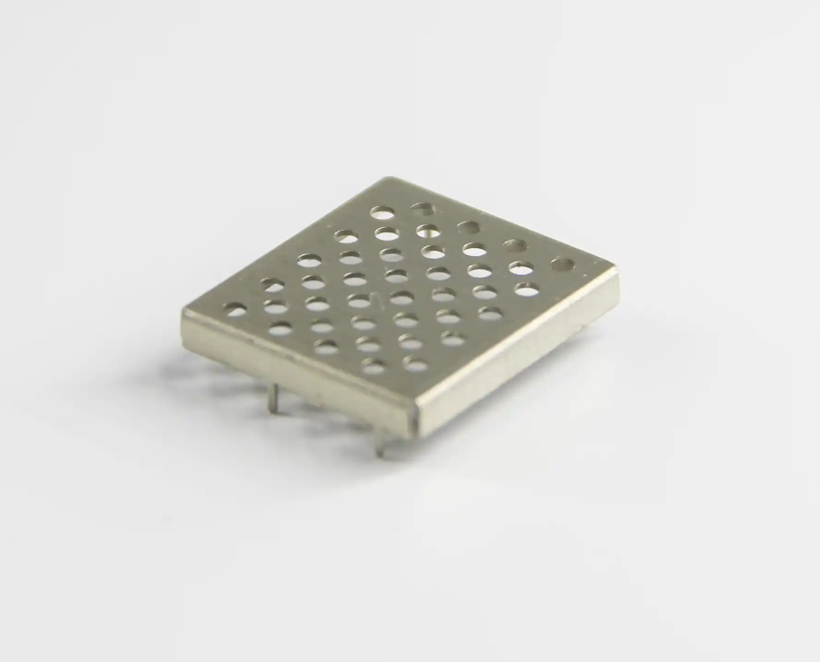
Record why each opening is present and which drawing controls its size and position. If a hole is intended for access, compare it with the actual component or tool envelope. If the purpose is not confirmed, leave it unresolved rather than calling the pattern ventilation. A clear photo does not provide a hole diameter, a pitch tolerance or a suitable operating-frequency range.
Leader Tech discusses how apertures and gaps at shield corners or internal interfaces can affect assembled shielding. That general guidance is a reason to refer an opening change to the responsible electrical design reviewer, not a basis for assigning an attenuation figure to this pictured cover. Keep the required test configuration and acceptance criterion explicit.
State what locates the cover in the assembly. A height measured from an arbitrary loose-part edge may not answer whether the installed cover clears the board components. Identify the board reference, seating features, orientation and component envelope on the controlled drawing. Include nearby connectors or other features only where they are part of the actual assembly.
If the cover is inspected in a fixture, record what the fixture constrains. Do not force a part into a mating condition and then report that result as its free-state shape. Conversely, a free-state measurement does not by itself establish installed clearance. Agree which condition applies to each critical characteristic before sample review.
TE Connectivity distinguishes one-piece and two-piece shields and lists separate mounting, locking and contact features. Those options are not interchangeable evidence of this part configuration. The real example shows projecting tabs; it does not establish a removable frame, solder joint, PCB hole fit or verified electrical bond.
Name the actual attachment method and the mating pad, hole or mechanical feature. If the same interface must carry a grounding function, identify who specifies and verifies that function after assembly. Acceptance of a tab dimension alone must not be reported as acceptance of the electrical path.
| Review record | What it should identify | What it does not establish alone |
|---|---|---|
| Loose-cover inspection | Drawing revision, selected dimensions, references, condition and edge requirements | Installed component clearance or system shielding performance |
| Assembly fit review | Actual board interface, locating features, installed condition and clearance evidence | EMC compliance or a validated grounding path |
| Electrical validation | Responsible reviewer, configuration, frequency or other specified scope, method and acceptance criteria | Conformity of every manufactured part or future drawing revision |
For a revision, list the changed aperture, wall or attachment features and decide which of these records must be updated. Do not carry an earlier assembly or test conclusion into a changed configuration without an explicit review. These are planning distinctions, not a claim that Zhengna Technology has performed the listed tests on the pictured part.
See the real PCB shielding cover and drawing-based supply scope. For the wider manufacturing family, see custom stamping parts. Send the controlled drawing and interface questions to Zhengna Technology; identify missing material, finish or acceptance requirements rather than filling them with catalogue assumptions.
Technical context: Leader Tech aperture guidance and TE Connectivity board-level shielding features. Their product-specific dimensions and performance figures are not Zhengna Technology specifications. Published by Zhengna Technology; no named expert review or test result is asserted.

 EN