Precision Stamping Parts for Electronics - High-Quality Metal Components for Electronic Applications

All Categories

Get a Free Quote

Our representative will contact you soon.
Email
Mobile/WhatsApp
Name
Company Name
Message
0/1000

precision stamping parts for electronics

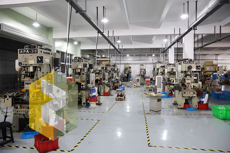
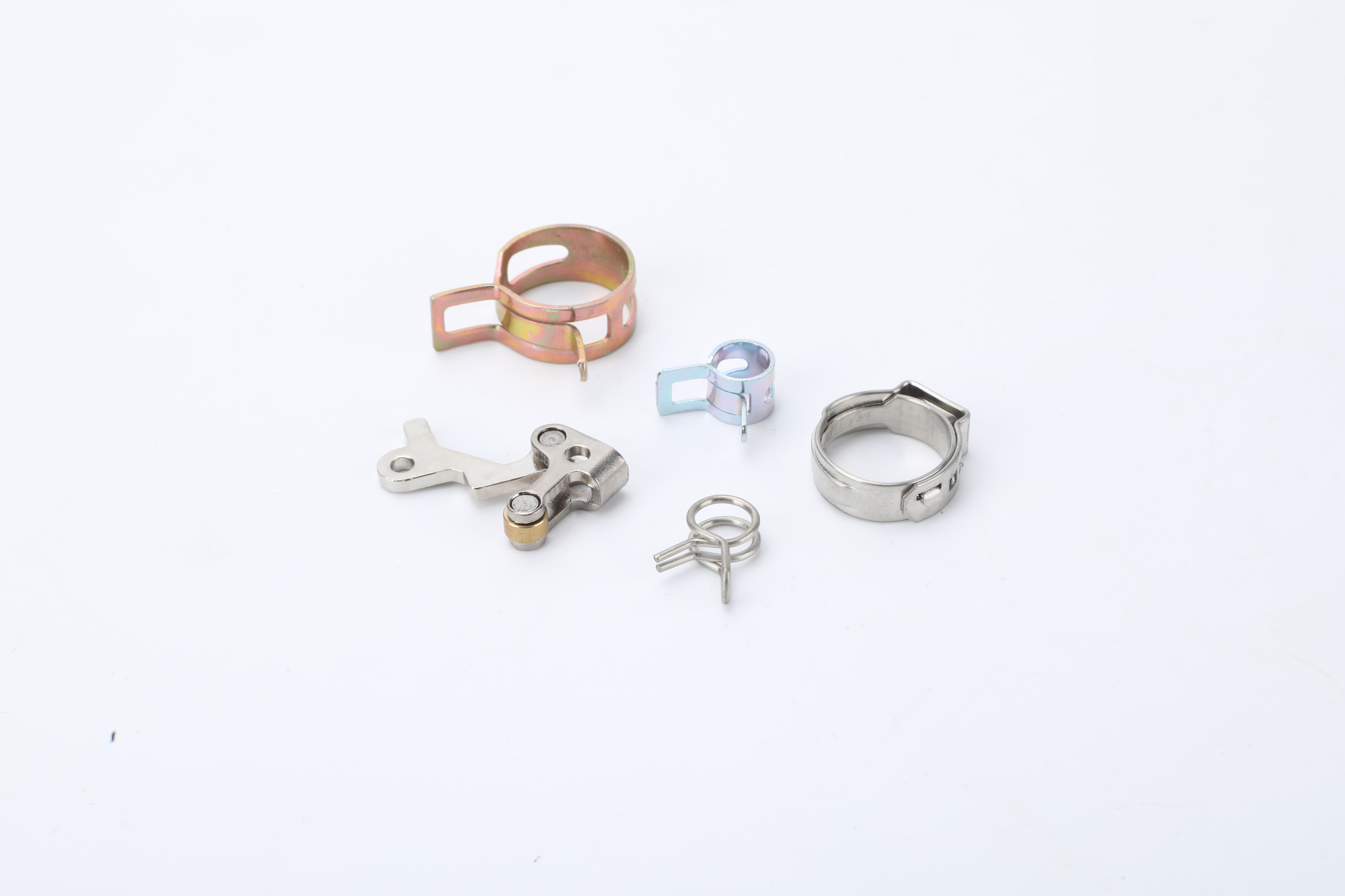
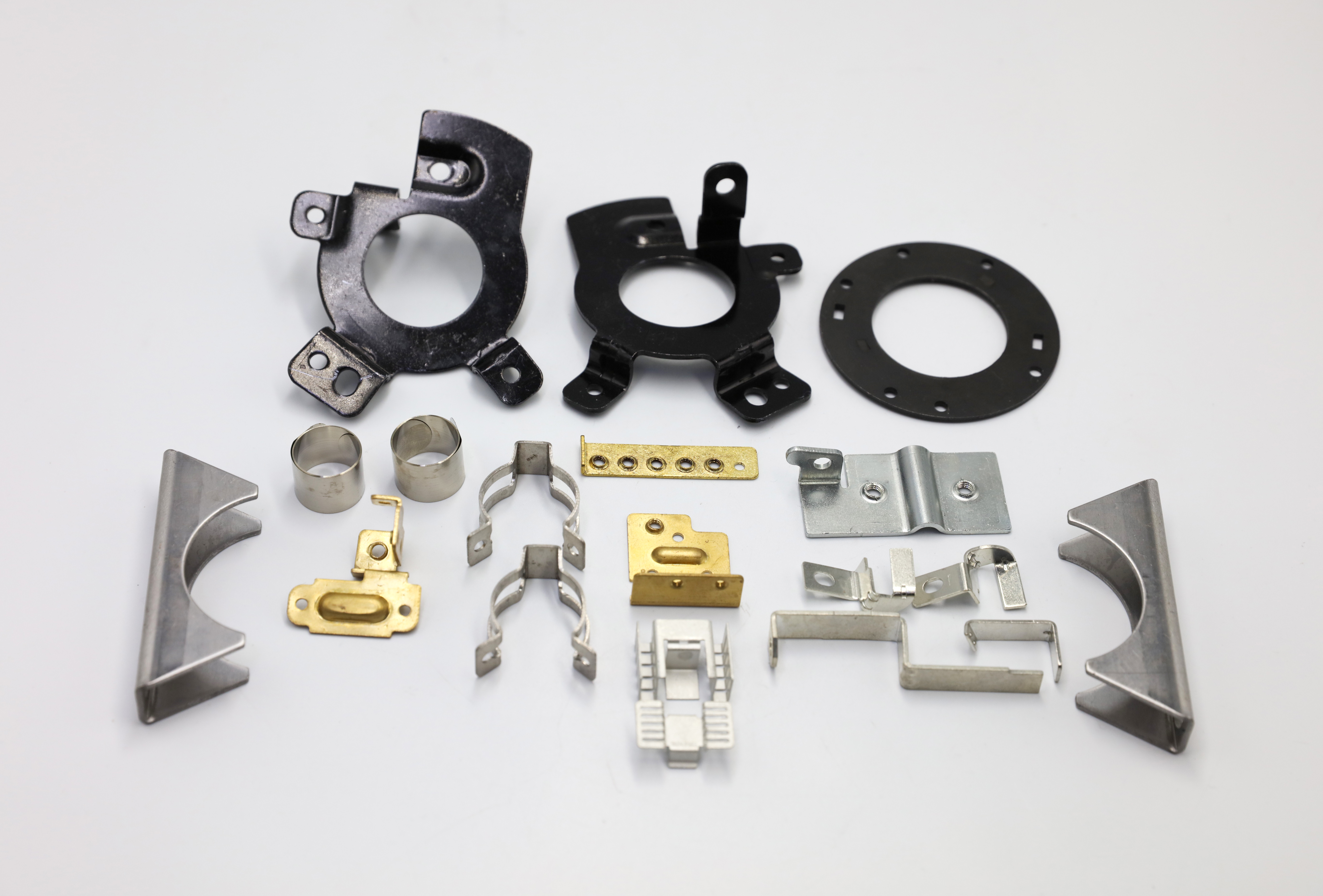
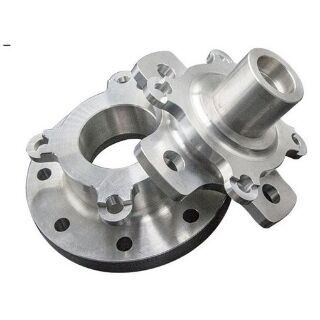
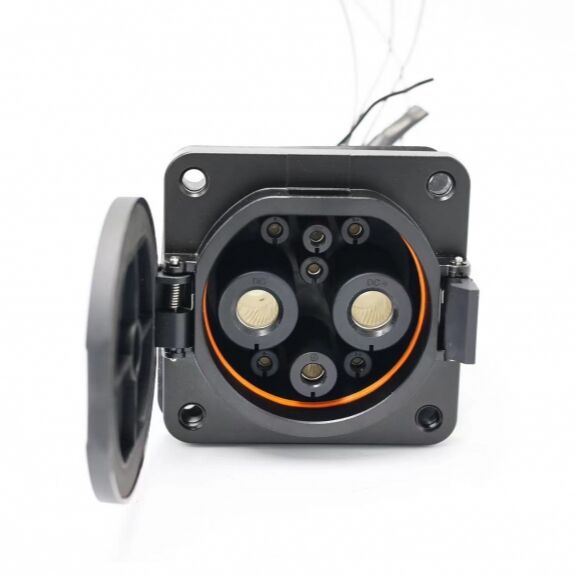
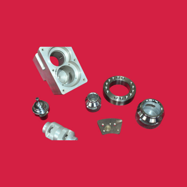
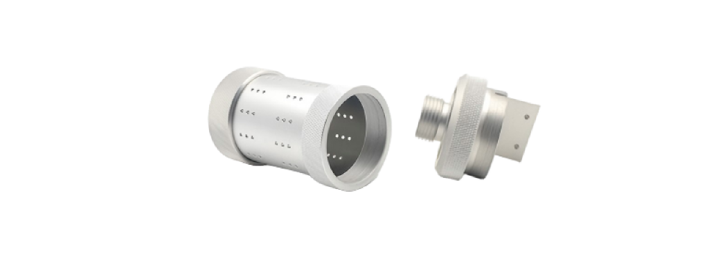
Precision stamping parts for electronics represent a cornerstone of modern manufacturing technology, delivering critical components that power today's sophisticated electronic devices. These meticulously crafted components undergo advanced metal forming processes that transform raw materials into precisely engineered parts with exceptional dimensional accuracy and surface quality. The manufacturing process involves sophisticated tooling systems that apply controlled force to metal sheets, creating complex geometries and intricate features required for electronic applications. Precision stamping parts for electronics serve multiple essential functions within electronic assemblies, including providing structural support, establishing electrical connections, ensuring proper component spacing, and facilitating heat dissipation. The technological features of these components encompass tight dimensional tolerances typically ranging from ±0.001 to ±0.005 inches, superior surface finishes that enhance conductivity and corrosion resistance, and material properties optimized for electronic applications. Advanced stamping techniques enable the production of complex three-dimensional shapes, fine-pitch connectors, and miniaturized components that meet the demanding requirements of modern electronics. These precision stamping parts for electronics find extensive applications across diverse sectors including consumer electronics, automotive systems, telecommunications infrastructure, medical devices, and industrial automation equipment. In smartphones and tablets, these components form critical elements such as battery contacts, shielding components, and connector assemblies that ensure reliable device operation. Automotive electronics rely heavily on precision stamped parts for engine control modules, infotainment systems, and safety-critical applications where performance and reliability are paramount. The manufacturing process incorporates advanced quality control measures, including statistical process control, automated inspection systems, and material traceability protocols that guarantee consistent part quality and performance. Modern production facilities utilize progressive die stamping, fine blanking, and micro-stamping technologies to achieve the exacting specifications required for electronic applications, ensuring that each precision stamping part meets the stringent demands of contemporary electronic systems.

New Products

Precision stamping parts for electronics deliver numerous compelling advantages that make them the preferred choice for manufacturers seeking reliable, cost-effective solutions for their electronic assemblies. The primary benefit lies in their exceptional dimensional accuracy, which ensures consistent fit and function across high-volume production runs, eliminating costly assembly issues and reducing field failures. This precision translates directly into improved product reliability and customer satisfaction, as electronic devices perform more consistently when equipped with properly manufactured stamped components. Cost efficiency represents another significant advantage, as precision stamping processes enable high-speed production of complex parts at substantially lower per-unit costs compared to alternative manufacturing methods such as machining or casting. The economies of scale achieved through stamping allow manufacturers to produce large quantities of precision stamping parts for electronics while maintaining competitive pricing structures that benefit both producers and end consumers. Material optimization capabilities inherent in the stamping process minimize waste generation, contributing to sustainable manufacturing practices and reduced environmental impact. The versatility of precision stamping accommodates a wide range of materials including copper alloys, stainless steel, aluminum, and specialized electronic-grade metals, enabling designers to select optimal materials for specific applications without manufacturing constraints. Surface quality advantages include consistent finishes that enhance electrical conductivity, improve corrosion resistance, and facilitate reliable soldering or welding operations during assembly processes. The rapid production speeds achievable with modern stamping equipment support tight delivery schedules and just-in-time manufacturing strategies, helping electronics manufacturers respond quickly to market demands and reduce inventory carrying costs. Quality consistency represents a crucial advantage, as precision stamping parts for electronics maintain uniform specifications across entire production batches, eliminating the variation often associated with other manufacturing processes. The ability to incorporate multiple features into single stamped parts reduces assembly complexity, lowers labor costs, and minimizes potential failure points in electronic systems. Advanced tooling capabilities enable the creation of complex geometries and fine details that would be challenging or impossible to achieve through alternative manufacturing methods, expanding design possibilities for electronics engineers and product developers.

Practical Tips

How To Determine The Chemical Stability Of Materials

10

Mar

How To Determine The Chemical Stability Of Materials

View More
How To Choose Appropriate Automotive Parts According To Testing Standards

10

Mar

How To Choose Appropriate Automotive Parts According To Testing Standards

View More

Get a Free Quote

Our representative will contact you soon.
Email
Mobile/WhatsApp
Name
Company Name
Message
0/1000

precision stamping parts for electronics

Superior Dimensional Accuracy and Repeatability

Superior Dimensional Accuracy and Repeatability

The exceptional dimensional accuracy achieved through precision stamping parts for electronics manufacturing represents a fundamental advantage that directly impacts product performance and manufacturing efficiency. This superior accuracy stems from advanced tooling technologies and sophisticated process control systems that maintain tolerances as tight as ±0.001 inches across millions of production cycles. The repeatability of these processes ensures that every stamped component meets identical specifications, eliminating the variation that can compromise electronic system performance and reliability. Modern stamping operations utilize computer-controlled servo presses that deliver precise force application and positioning accuracy, enabling the production of components with consistent wall thickness, hole diameters, and feature locations that are critical for proper electrical connections and mechanical assembly. The dimensional stability of precision stamping parts for electronics extends beyond initial production to include long-term performance characteristics, as properly stamped components maintain their geometric integrity under various operating conditions including temperature cycling, mechanical stress, and environmental exposure. Advanced measurement and inspection systems integrated into the manufacturing process provide real-time feedback that enables immediate corrections to maintain dimensional accuracy throughout extended production runs. This level of precision proves particularly valuable in miniaturized electronic applications where space constraints demand components that fit together with minimal clearance and perfect alignment. The economic benefits of superior dimensional accuracy include reduced assembly time, lower rejection rates, and decreased warranty costs associated with field failures caused by dimensional variations. Quality assurance protocols incorporate statistical process control methodologies that track dimensional parameters across time, ensuring consistent output quality and enabling predictive maintenance of tooling systems. The precision achieved through modern stamping processes eliminates the need for secondary operations such as machining or grinding in many applications, reducing production costs and lead times while maintaining the exacting standards required for electronic applications. This dimensional excellence enables electronics manufacturers to implement automated assembly processes with confidence, knowing that precision stamping parts for electronics will consistently meet the tight tolerances required for robotic handling and placement systems.
Enhanced Material Properties and Performance Characteristics

Enhanced Material Properties and Performance Characteristics

The enhanced material properties achieved through precision stamping processes for electronics applications deliver significant performance advantages that extend far beyond basic dimensional requirements. The controlled deformation process inherent in precision stamping work-hardens materials in beneficial ways, increasing strength and durability while maintaining the electrical and thermal properties essential for electronic applications. This work hardening effect creates components with superior fatigue resistance and mechanical stability compared to parts produced through alternative manufacturing methods, ensuring long-term reliability in demanding electronic environments. Precision stamping parts for electronics benefit from optimized grain structure alignment that occurs during the forming process, resulting in improved electrical conductivity and reduced resistance characteristics that are crucial for high-performance electronic connections. The surface integrity achieved through precision stamping includes consistent surface roughness and minimal subsurface damage, creating ideal conditions for subsequent finishing operations such as plating, coating, or surface treatments that enhance corrosion resistance and solderability. Material utilization efficiency reaches optimal levels through advanced nesting algorithms and progressive die designs that minimize waste while maximizing the number of parts produced from each sheet of raw material, contributing to cost reduction and environmental sustainability. The stress distribution patterns created during precision stamping can be engineered to enhance specific performance characteristics such as spring properties in contact elements or flexibility in connector components, enabling designers to optimize component behavior for specific applications. Precision stamping parts for electronics manufactured from specialized alloys maintain their metallurgical properties throughout the forming process, preserving characteristics such as magnetic permeability, thermal conductivity, and electrical resistivity that are critical for electronic function. The controlled heating and cooling cycles associated with some stamping operations can be used to achieve specific material conditions such as stress relief or precipitation hardening, further enhancing component performance and reliability. Edge quality represents another significant advantage, as precision stamping produces clean, burr-free edges that eliminate the need for secondary deburring operations while ensuring safe handling during assembly processes. The material properties achieved through precision stamping enable components to meet stringent industry standards and certifications required for electronic applications, including automotive, aerospace, and medical device sectors where performance and reliability are non-negotiable requirements.
Cost-Effective High-Volume Production Capabilities

Cost-Effective High-Volume Production Capabilities

The cost-effectiveness of precision stamping parts for electronics production becomes increasingly advantageous as volume requirements increase, making this manufacturing method the preferred choice for high-volume electronic component production. The fundamental economics of stamping operations favor large production runs, as the initial tooling investment is amortized across millions of parts, resulting in extremely competitive per-unit costs that alternative manufacturing methods cannot match. Progressive die stamping systems enable the simultaneous execution of multiple operations within a single press stroke, dramatically reducing production time and labor costs while maintaining the precision required for electronic applications. The automation capabilities inherent in modern stamping operations minimize direct labor requirements and eliminate human error factors that can impact quality and consistency, resulting in lower operational costs and improved profit margins for electronics manufacturers. Precision stamping parts for electronics production benefits from rapid changeover capabilities that enable manufacturers to switch between different part configurations quickly and efficiently, supporting diverse product lines and customization requirements without significant downtime or setup costs. The scalability of stamping operations allows manufacturers to adjust production volumes rapidly in response to market demands, providing the flexibility needed to support seasonal fluctuations and product lifecycle management strategies common in the electronics industry. Material efficiency advantages include optimized blank layouts and minimal scrap generation, contributing to lower raw material costs and reduced waste disposal expenses that impact overall production economics. The reliability and consistency of precision stamping processes reduce quality-related costs including inspection time, rework expenses, and warranty claims, improving overall profitability and customer satisfaction metrics. Energy efficiency represents another cost advantage, as modern stamping presses consume significantly less energy per part compared to alternative manufacturing methods such as machining or molding, contributing to lower operational costs and environmental compliance objectives. The longevity of properly designed and maintained stamping dies enables extended production runs without significant tooling replacement costs, further improving the economic attractiveness of precision stamping parts for electronics applications. Supply chain advantages include shorter lead times and reduced inventory requirements, as the rapid production capabilities of stamping operations support just-in-time delivery strategies that minimize carrying costs and improve cash flow management for electronics manufacturers.

Get a Free Quote

Our representative will contact you soon.
Email
Mobile/WhatsApp
Name
Company Name
Message
0/1000