
High-speed telecommunication gear operates in an environment where milliseconds matter and signal integrity cannot be compromised. The infrastructure supporting 5G networks, fiber-optic routers, base station equipment, and microwave transmission systems depends on components that deliver exceptional dimensional accuracy, electrical conductivity, and mechanical reliability. Among these critical components, precision stamping parts serve as the foundational hardware enabling seamless data transmission, robust electromagnetic shielding, and thermal management across telecommunication platforms. Without the exacting tolerances and material consistency provided by precision stamping parts, modern telecommunication systems would suffer from signal degradation, increased downtime, and catastrophic performance failures under high-frequency operational demands.
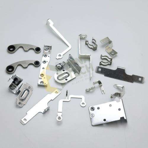
The essential role of precision stamping parts in high-speed telecommunication gear stems from their unique ability to meet stringent electrical, mechanical, and thermal requirements simultaneously. These stamped components—including EMI shielding frames, PCB grounding clips, RF connector housings, and heat dissipation brackets—are manufactured through progressive die stamping processes that achieve tolerances often within ±0.02mm. This level of precision directly impacts signal path continuity, impedance matching, and thermal interface efficiency, all of which determine whether telecommunication equipment can sustain gigabit-per-second data rates without packet loss or latency spikes. As network operators transition to higher frequencies and denser equipment configurations, the demand for precision stamping parts with advanced material properties and defect-free surface finishes has become non-negotiable.
The Critical Performance Demands of High-Speed Telecommunication Infrastructure
Signal Integrity Requirements in Multi-Gigahertz Operating Environments
Telecommunication equipment operating at frequencies above 20 GHz experiences signal behaviors that demand ultra-precise component geometry. Even microscopic variations in connector pin alignment, shielding gap width, or grounding contact pressure can introduce impedance mismatches that reflect RF energy back into the signal path. Precision stamping parts address these challenges by maintaining dimensional consistency across millions of production cycles, ensuring that every shielding can, spring contact, or mounting bracket performs identically. The surface roughness of stamped metal contacts directly affects insertion loss and return loss parameters measured in dB—critical metrics for 5G base stations and millimeter-wave transmission equipment where signal budgets are exceptionally tight.
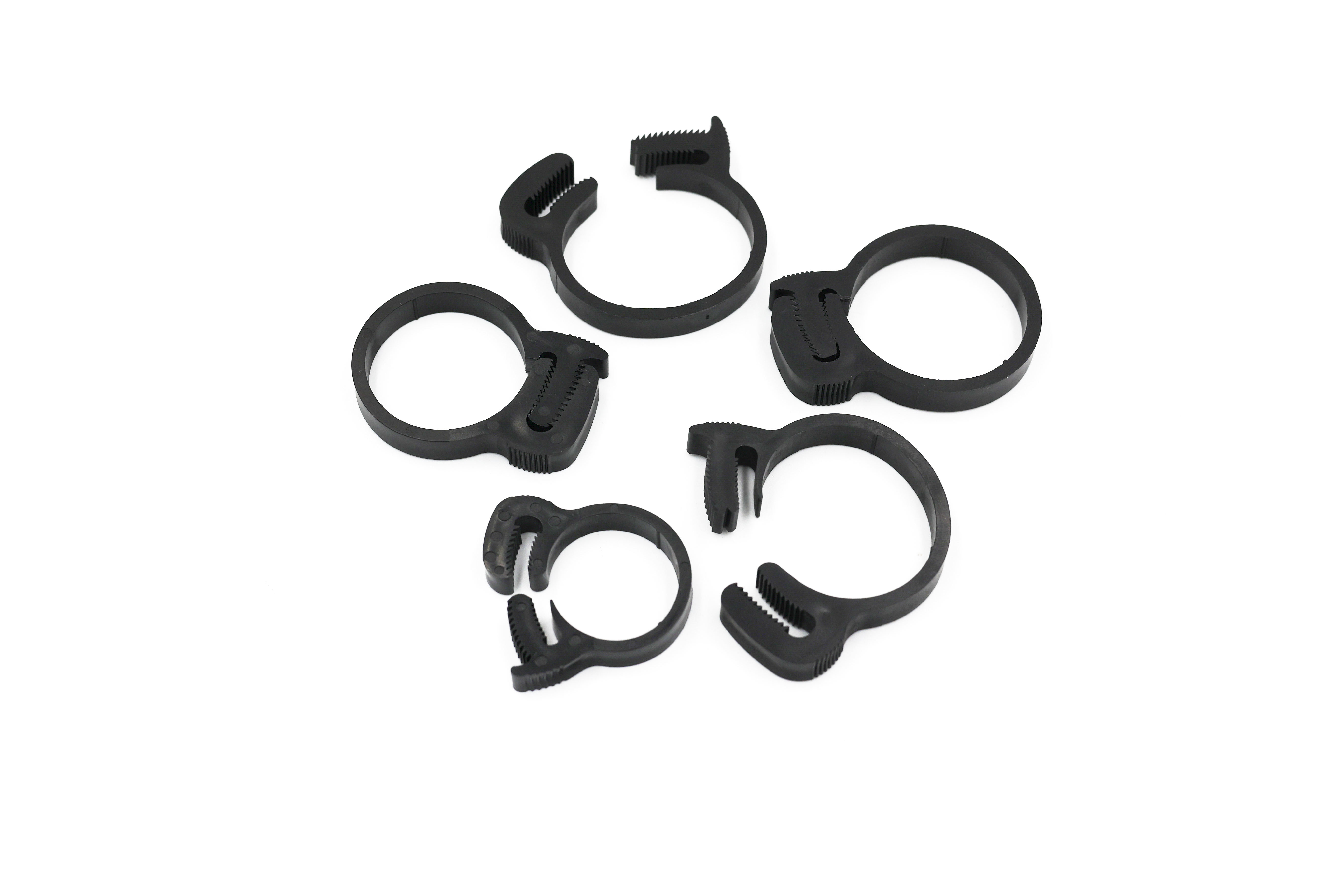
Unlike machined or fabricated components, precision stamping parts can achieve burr-free edges and controlled surface finishes through integrated secondary operations within the stamping die itself. This capability is essential for RF shielding enclosures where any protruding edge acts as an antenna, radiating electromagnetic interference that disrupts adjacent circuits. The progressive stamping process enables manufacturers to incorporate bending, coining, and embossing features that enhance electrical contact reliability while minimizing material waste. For high-speed telecommunication gear, where hundreds of interconnect points exist within a single line card assembly, the cumulative effect of using precision stamping parts versus lower-tolerance alternatives translates to measurably superior bit error rates and system uptime.
Thermal Management Constraints in High-Density Equipment Racks
Modern telecommunication facilities deploy equipment racks where power density can exceed 15 kilowatts per rack unit, generating heat loads that threaten component lifespan and performance stability. Precision stamping parts fabricated from copper alloys, aluminum, or specialized thermal interface materials serve as heat sinks, thermal spreaders, and mounting brackets that conduct heat away from critical RF amplifiers, optical transceivers, and signal processors. The flat, uniform contact surfaces achieved through precision stamping ensure maximum thermal coupling between heat-generating chips and cooling infrastructure, reducing junction temperatures by 10 to 20 degrees Celsius compared to poorly fitted hardware.
The material selection for precision stamping parts in thermal management applications involves careful consideration of thermal conductivity, coefficient of thermal expansion, and long-term creep resistance. Telecommunication gear must operate continuously for years in environments ranging from climate-controlled data centers to outdoor cabinets exposed to temperature swings exceeding 80 degrees Celsius. Precision stamping parts manufactured from phosphor bronze or beryllium copper alloys maintain spring tension and contact pressure across these temperature extremes, preventing thermal runaway conditions that lead to equipment shutdowns. The ability to stamp complex fin geometries, ventilation grilles, and heat pipe mounting brackets with repeatable accuracy makes this manufacturing method indispensable for next-generation telecommunication hardware design.
Electromagnetic Compatibility Standards and Shielding Effectiveness
Regulatory compliance with EMC standards such as FCC Part 15, ETSI EN 301 489, and CISPR 22 requires telecommunication equipment to limit radiated and conducted emissions while maintaining immunity to external interference. Precision stamping parts form the physical barriers that contain electromagnetic fields within designated enclosures and prevent crosstalk between adjacent signal paths. Shielding cans, gaskets, and grounding fingers must maintain electrical continuity with chassis ground across all mounting points, a requirement that demands both dimensional precision and surface conductivity. Any gap wider than one-tenth of the operating wavelength compromises shielding effectiveness, allowing RF energy to leak into sensitive receiver circuits or radiate beyond equipment boundaries.
The design of precision stamping parts for EMI shielding applications incorporates features such as multiple contact points, compliant spring fingers, and coined grounding surfaces that ensure low impedance paths even under vibration or thermal cycling. Telecommunication gear deployed in mobile base stations or vehicle-mounted systems experiences mechanical shock and sustained vibration that can degrade shielding performance if hardware lacks proper retention force. Precision stamping processes enable the integration of self-clinching fasteners, captive clips, and interference-fit tabs directly into shielding components, eliminating the need for secondary assembly operations that introduce variability. This manufacturing approach results in shielding effectiveness levels exceeding 80 dB at frequencies up to 10 GHz, meeting the stringent requirements of both commercial and military telecommunication applications.
Manufacturing Advantages Unique to Precision Stamping Technology
Dimensional Tolerance Capabilities and Process Repeatability
The economic viability of high-volume telecommunication equipment production depends on component suppliers delivering millions of parts with identical specifications. Precision stamping parts achieve this through progressive die systems where each station performs a specific forming operation—piercing, bending, embossing, or blanking—with positional accuracy maintained by pilot pins and die guide systems. Modern stamping presses equipped with servo-driven slide motion and real-time die protection sensors can detect thickness variations, material hardness changes, and tool wear before defective parts reach the customer. This level of process control ensures that critical dimensions such as pin spacing in connector housings or slot width in ventilation panels remain within ±0.03mm across production runs spanning multiple years.
The repeatability of precision stamping parts directly impacts the automated assembly processes used in telecommunication manufacturing. Pick-and-place robots, wave soldering systems, and automated optical inspection equipment all depend on components arriving with predictable geometry and surface condition. Stamped parts with consistent hole locations enable vision-guided assembly systems to achieve placement accuracies within 0.05mm, critical for surface-mount connector interfaces and coaxial cable terminations. The elimination of manual fitting, rework, and quality inspection delays reduces overall equipment assembly costs by 15 to 25 percent compared to fabrication methods requiring secondary machining or hand finishing operations.
Material Utilization Efficiency and Supply Chain Optimization
Telecommunication equipment manufacturers face pressure to reduce both material costs and environmental impact while maintaining performance standards. Precision stamping parts achieve material utilization rates exceeding 70 percent through optimized strip layout designs that nest multiple part geometries within a single coil of sheet metal. Advanced nesting algorithms minimize scrap generation by positioning parts to share common edges and utilize material between mounting holes for adjacent components. This efficiency becomes critical when working with expensive alloys such as beryllium copper, which costs three to five times more than standard brass but offers superior spring properties and electrical conductivity required for high-speed telecommunication gear.
The supply chain advantages of precision stamping parts extend beyond raw material savings to include inventory management and logistics optimization. Stamped components can be produced in continuous coil form, automatically packaged in carrier tape, and shipped in compact reels compatible with automated assembly feeders. This packaging format reduces handling damage, simplifies inventory tracking, and enables just-in-time delivery schedules that minimize working capital requirements. For telecommunication equipment manufacturers operating global supply chains, the ability to source precision stamping parts from qualified suppliers with consistent tooling standards ensures production continuity even when switching between regional fabrication partners during capacity constraints or geopolitical disruptions.
Integration of Secondary Operations Within the Stamping Process
The versatility of precision stamping technology allows manufacturers to incorporate value-added operations directly within the progressive die sequence, eliminating secondary processes that add cost and lead time. Telecommunication hardware often requires precision stamping parts with threaded features, clinched inserts, welded studs, or plated surfaces—all of which can be integrated into the stamping line through in-die tapping, insert feeding, projection welding stations, or selective plating fixtures. This consolidation reduces handling steps, prevents positional tolerance stack-up errors, and ensures that all features maintain proper alignment relative to the base part geometry.
Surface finishing operations such as tin plating, gold plating, or nickel plating can be applied to precision stamping parts through continuous reel-to-reel electroplating systems that process stamped components while still attached to the carrier strip. This approach provides uniform coating thickness across complex three-dimensional geometries, critical for maintaining low contact resistance in spring finger assemblies and connector pins. The ability to selectively plate only contact areas while leaving structural regions bare reduces precious metal consumption without compromising electrical performance. For high-speed telecommunication gear where thousands of plated contacts exist within a single equipment chassis, this cost optimization strategy delivers material savings exceeding 30 percent compared to fully plated alternatives while maintaining identical signal integrity performance.
Application-Specific Design Considerations for Telecommunication Hardware
RF Connector Housing and Contact System Requirements
The performance of high-frequency RF connectors used in telecommunication gear depends entirely on the precision of stamped contact systems that maintain consistent impedance along the signal path. Precision stamping parts such as center conductors, outer shell segments, and dielectric retention fingers must achieve positional tolerances within 0.01mm to prevent impedance discontinuities that generate reflections and insertion loss. The spring force characteristics of stamped contacts must remain stable across hundreds of mating cycles while maintaining contact resistance below 5 milliohms to preserve signal quality at frequencies extending into the millimeter-wave spectrum.
Connector manufacturers rely on precision stamping parts fabricated from beryllium copper alloys that combine high electrical conductivity with excellent spring properties and resistance to stress relaxation. The stamping process enables the creation of complex beam geometries with multiple contact points, distributed normal force, and controlled wiping action that breaks through surface oxides during mating. These design features ensure that RF connectors maintain performance specifications even after exposure to temperature cycling, vibration, and corrosive atmospheres encountered in outdoor telecommunication installations. The dimensional consistency of precision stamping parts allows connector suppliers to guarantee VSWR performance better than 1.2:1 across production volumes exceeding one million units—a requirement impossible to meet with manually adjusted or machined contact systems.
PCB Grounding and EMI Suppression Hardware
Circuit boards within telecommunication equipment require numerous grounding points to prevent ground loops, reduce common-mode noise, and provide low-impedance return paths for high-frequency signals. Precision stamping parts such as board-level shields, grounding clips, and spring fingers establish electrical continuity between PCB ground planes and chassis structures while accommodating manufacturing tolerances in board thickness, warpage, and component height variations. The spring rate and contact geometry of these stamped components must be carefully optimized to provide sufficient normal force without damaging sensitive printed circuit board surfaces or solder mask coatings.
The effectiveness of precision stamping parts in EMI suppression applications depends on maintaining multiple contact points distributed along shield perimeters to prevent slot antenna effects that radiate electromagnetic energy. Advanced stamping designs incorporate coined contact dimples, formed spring fingers, and offset mounting tabs that ensure consistent contact pressure even when PCB assemblies undergo thermal expansion during operation. For high-speed telecommunication gear operating with clock frequencies exceeding 10 GHz, the inductance of grounding paths must remain below 1 nanohenry to prevent ground bounce phenomena that corrupt digital signal timing. Precision stamping parts achieve this performance level through minimal lead lengths, direct chassis contact, and optimized current distribution across multiple parallel paths—design features difficult or impossible to replicate with wire bonding or threaded fastener approaches.
Thermal Interface Mounting and Heat Dissipation Structures
Power amplifiers, optical transceivers, and signal processing ASICs within telecommunication equipment generate heat flux densities approaching 100 watts per square centimeter, requiring precision stamping parts that serve as thermal interfaces between semiconductor packages and forced-air or liquid cooling systems. Mounting brackets, heat sink clips, and thermal spreader plates must provide uniform clamping force across chip surfaces while maintaining flatness tolerances within 0.05mm to ensure proper thermal interface material compression. Any air gap or uneven pressure distribution increases thermal resistance, elevating junction temperatures beyond safe operating limits and reducing component lifespan.
The design of precision stamping parts for thermal management applications incorporates features such as coined mounting pads, formed spring elements, and captive fastener integration that simplify assembly while guaranteeing proper installation torque and alignment. Stamped heat sink mounting clips manufactured from spring steel or stainless steel alloys maintain retention force across temperature cycling without stress relaxation, preventing thermal runaway conditions caused by loosened hardware. The ability to stamp complex fin arrays, ventilation louvers, and airflow directing baffles enables thermal engineers to optimize cooling efficiency within the tight spatial constraints of high-density telecommunication equipment racks. These precision stamping parts contribute directly to achieving thermal design power targets while minimizing fan speeds, acoustic noise, and overall system energy consumption.
Quality Assurance and Testing Protocols for Mission-Critical Applications
Dimensional Inspection and Statistical Process Control Methods
Telecommunication equipment manufacturers impose rigorous inspection requirements on precision stamping parts suppliers to ensure consistent quality across multi-year production contracts. Coordinate measuring machines equipped with optical probes and laser scanners verify critical dimensions, surface profiles, and feature positions against CAD models with measurement uncertainty below 2 microns. Statistical process control charts track key characteristics such as hole diameter, bend angle, and material thickness across production lots, triggering corrective actions when process capability indices fall below 1.67—a threshold ensuring defect rates remain under 10 parts per million.
Advanced quality systems for precision stamping parts incorporate automated optical inspection integrated directly into stamping press operations, capturing high-resolution images of every part at full production speed. Machine vision algorithms trained on deep learning models detect surface defects, dimensional deviations, and material defects with accuracy exceeding manual inspection while generating complete traceability records linked to specific die cavities and material lot numbers. This real-time quality monitoring capability enables suppliers to identify and correct tooling wear, material inconsistencies, or process drift before defective precision stamping parts reach telecommunication equipment assembly lines where they would cause expensive production delays and field failures.
Electrical Performance Validation and Contact Resistance Testing
The electrical characteristics of precision stamping parts used in high-speed telecommunication gear require verification through specialized testing protocols that measure contact resistance, spring force, insertion loss, and shielding effectiveness under conditions simulating actual service environments. Four-wire Kelvin measurement systems quantify contact resistance with micro-ohm resolution across temperature ranges spanning -40 to +85 degrees Celsius, ensuring that stamped contacts maintain low impedance connections throughout equipment operating specifications. Spring force testing using calibrated load cells validates that stamped contacts generate sufficient normal force to penetrate surface oxides and maintain stable electrical interfaces across hundreds of mating cycles.
RF performance testing of precision stamping parts intended for connector applications employs vector network analyzers measuring S-parameters from DC to 67 GHz, characterizing insertion loss, return loss, and phase linearity against industry standards. Shielding effectiveness testing places stamped enclosures within calibrated test chambers illuminated by known electromagnetic field strengths, measuring transmitted power levels to verify attenuation performance meets specification requirements. These comprehensive electrical validation protocols ensure that precision stamping parts deliver consistent performance across production volumes while identifying material quality issues, plating defects, or dimensional variations that compromise signal integrity in deployed telecommunication systems.
Environmental Stress Testing and Reliability Qualification
Telecommunication equipment deployed in base stations, central offices, and remote cabinets must operate reliably for decades despite exposure to temperature extremes, humidity, vibration, and atmospheric contaminants. Precision stamping parts undergo accelerated life testing including thermal cycling between -55 and +125 degrees Celsius, salt fog exposure per ASTM B117, and vibration profiles matching MIL-STD-810 requirements. These environmental stress protocols validate that stamped components maintain dimensional stability, spring force retention, and surface finish integrity throughout anticipated service lifetimes exceeding 100,000 operating hours.
Corrosion resistance testing assumes critical importance for precision stamping parts fabricated from copper alloys susceptible to tarnishing, oxidation, or dezincification when exposed to sulfur compounds, chlorides, or industrial atmospheres. Protective plating systems such as tin-over-nickel or gold-over-nickel undergo porosity testing, adhesion testing, and accelerated corrosion exposure to ensure long-term contact reliability. For telecommunication applications where field replacement of failed hardware incurs substantial labor costs and service disruption penalties, the reliability of precision stamping parts directly impacts total cost of ownership and customer satisfaction metrics. Suppliers demonstrating superior environmental stress performance through comprehensive qualification testing secure preferred vendor status and long-term supply agreements with major telecommunication equipment manufacturers.
Future Technology Trends Driving Precision Stamping Innovation
Millimeter-Wave Frequency Requirements and Material Advances
The expansion of 5G networks into millimeter-wave frequency bands between 24 and 86 GHz imposes unprecedented demands on precision stamping parts supporting antenna systems, waveguide transitions, and RF front-end modules. At these frequencies, wavelengths shrink to millimeters, making every dimensional tolerance, surface roughness specification, and material loss tangent critical to system performance. Precision stamping parts for mmWave applications require surface finishes smoother than 0.4 microns Ra and positional tolerances approaching ±0.01mm to prevent signal reflections and mode conversion losses that degrade link budgets already challenged by atmospheric absorption and rain fade.
Material science advances enable precision stamping parts fabricated from copper alloys with enhanced electrical conductivity approaching 100 percent IACS or specialized composites combining mechanical strength with low dielectric loss properties. Stamped components serving as waveguide flanges, antenna mounting brackets, and RF shield enclosures must maintain electrical performance specifications across frequency ranges where skin effect confines current flow to surface layers thinner than 1 micron. The development of plating processes depositing silver or gold layers with controlled grain structure and minimal surface roughness ensures precision stamping parts meet insertion loss budgets measured in hundredths of a decibel—performance margins critical for maintaining millimeter-wave link reliability over distances exceeding 500 meters.
Integration with Advanced Assembly Technologies
Next-generation telecommunication equipment incorporates heterogeneous integration approaches combining silicon photonics, RF front-end modules, and digital signal processing circuits within compact multi-chip packages. Precision stamping parts enable these advanced architectures through innovative designs such as stamped lead frames with integrated heat spreaders, micro-spring arrays for fine-pitch interconnects, and formed cavities providing EMI isolation between functional blocks. The dimensional precision achievable through progressive die stamping supports automated assembly processes including flip-chip bonding, wire bonding, and thermocompression attachment where positioning accuracies must remain within 5 microns across thermal cycling and mechanical stress.
The convergence of precision stamping technology with additive manufacturing techniques creates hybrid components combining stamped base structures with 3D-printed features optimized for electromagnetic performance or thermal management. Telecommunication equipment designers leverage this approach to create customized precision stamping parts incorporating lattice structures for weight reduction, conformal cooling channels for thermal optimization, or metamaterial patterns for antenna beam shaping—all integrated within conventionally stamped frames maintaining high-volume manufacturability and cost efficiency. These manufacturing innovations position precision stamping parts as enabling technologies for sixth-generation wireless systems, satellite communication terminals, and quantum communication infrastructure requiring unprecedented levels of performance integration and reliability.
Sustainability Initiatives and Circular Economy Considerations
Environmental regulations and corporate sustainability commitments drive telecommunication equipment manufacturers toward designs incorporating recyclable materials, reduced energy consumption, and extended product lifespans. Precision stamping parts manufactured from readily recyclable metals such as copper, aluminum, and stainless steel support circular economy principles through material recovery rates exceeding 95 percent at end-of-life. The energy efficiency of stamping processes compared to subtractive machining or additive manufacturing reduces carbon footprint per component by 40 to 60 percent, contributing to scope 3 emissions reduction targets established by major network operators and equipment suppliers.
Design for disassembly principles influence precision stamping parts through features such as snap-fit retention, tool-free removal mechanisms, and material identification markings that simplify equipment refurbishment and component reuse. Telecommunication infrastructure upgrades increasingly prioritize modular architectures where precision stamping parts in chassis structures, thermal management systems, and connector interfaces remain serviceable across multiple technology generations. This approach extends useful life of capital equipment while reducing electronic waste volumes and material consumption associated with complete system replacements. The role of precision stamping parts in enabling sustainable telecommunication infrastructure positions this manufacturing technology as essential not only for technical performance but also for achieving environmental stewardship objectives demanded by regulators, investors, and end customers worldwide.
FAQ
What dimensional tolerances can precision stamping achieve for telecommunication components?
Modern precision stamping processes routinely achieve dimensional tolerances of ±0.025mm for critical features such as mounting hole positions, bend angles, and overall part dimensions. Advanced progressive dies equipped with pilot pin systems and servo-controlled presses can maintain tolerances as tight as ±0.01mm for specialized applications including RF connector contacts and EMI shielding components. These tolerance capabilities ensure that precision stamping parts meet the stringent requirements of high-speed telecommunication gear where signal integrity depends on consistent component geometry across millions of production units.
How do material choices affect the performance of stamped parts in telecommunication applications?
Material selection for precision stamping parts balances electrical conductivity, mechanical spring properties, corrosion resistance, and thermal management characteristics. Beryllium copper alloys provide optimal combination of high conductivity and spring force retention for connector contacts and grounding clips. Phosphor bronze offers excellent stress relaxation resistance for applications requiring sustained contact pressure across temperature cycling. Aluminum alloys serve thermal management roles where light weight and high thermal conductivity outweigh electrical performance requirements. Stainless steel grades provide corrosion resistance for outdoor telecommunication installations exposed to harsh environmental conditions. Each material choice directly impacts the reliability, longevity, and electrical performance of stamped components within high-speed communication systems.
What quality certifications should telecommunication equipment manufacturers require from stamping suppliers?
Suppliers of precision stamping parts for telecommunication applications should maintain ISO 9001 quality management certification as a baseline requirement, with additional certifications such as IATF 16949 demonstrating advanced process control capabilities. Environmental compliance certifications including ISO 14001 and RoHS conformity ensure stamped components meet material restriction requirements for global markets. Suppliers serving aerospace and defense telecommunication segments require AS9100 certification validating quality systems suitable for mission-critical applications. First article inspection reports, material certifications, and statistical process control documentation provide evidence that precision stamping parts meet specified tolerances, material properties, and performance characteristics essential for high-reliability telecommunication equipment.
Can precision stamping technology accommodate the miniaturization trends in telecommunication hardware?
Precision stamping processes excel at producing miniature components required by increasingly compact telecommunication equipment designs. Micro-stamping capabilities enable production of parts with features smaller than 0.3mm, including fine-pitch connector contacts, micro-spring arrays, and miniature EMI shielding components. Advanced die designs incorporating compound forming operations, micro-piercing, and fine blanking techniques maintain dimensional accuracy even as part sizes shrink below 5mm characteristic dimensions. The scalability of stamping technology from prototype quantities through multi-million piece production runs makes it ideal for supporting both initial product development and high-volume manufacturing of miniaturized telecommunication hardware components.
Table of Contents
- The Critical Performance Demands of High-Speed Telecommunication Infrastructure
- Manufacturing Advantages Unique to Precision Stamping Technology
- Application-Specific Design Considerations for Telecommunication Hardware
- Quality Assurance and Testing Protocols for Mission-Critical Applications
- Future Technology Trends Driving Precision Stamping Innovation
-
FAQ
- What dimensional tolerances can precision stamping achieve for telecommunication components?
- How do material choices affect the performance of stamped parts in telecommunication applications?
- What quality certifications should telecommunication equipment manufacturers require from stamping suppliers?
- Can precision stamping technology accommodate the miniaturization trends in telecommunication hardware?