
The electronics industry's relentless pursuit of cost optimization while maintaining quality has led manufacturers to examine every aspect of their production processes. Among the various manufacturing techniques available for electronic components, custom metal stamping has emerged as a dominant force, fundamentally changing how companies approach component fabrication. This manufacturing method addresses the critical challenge of producing high-volume electronic parts while keeping costs manageable and quality consistent.
Understanding why custom metal stamping delivers superior cost-effectiveness requires examining the unique economic dynamics of electronics manufacturing. Unlike traditional machining or fabrication methods that require extensive setup times and material waste, custom metal stamping leverages precision tooling to create consistent, repeatable results with minimal material loss. The economics become even more compelling when considering the volume requirements typical in electronics production, where thousands or millions of identical components must be manufactured to exact specifications.
Economic Advantages of Custom Metal Stamping in Electronics Production
Material Utilization Efficiency
Custom metal stamping achieves exceptional material utilization rates that directly impact the bottom line of electronics manufacturing. Traditional machining processes often result in material waste rates of 40-60%, where significant portions of raw material are removed as chips or scrap. In contrast, custom metal stamping typically achieves material utilization rates exceeding 85%, with some applications reaching 95% efficiency. This dramatic reduction in waste translates to immediate cost savings on raw materials, which represent a substantial portion of component costs in electronics manufacturing.
The precision of custom metal stamping dies ensures that each part utilizes exactly the required amount of material without excess. Progressive dies can create complex geometries while maintaining optimal material flow, minimizing scrap generation. For electronics components where precious metals like copper, silver, or specialized alloys are involved, this efficiency becomes even more critical from a cost perspective. The ability to nest multiple part geometries within a single sheet layout further enhances material utilization, allowing manufacturers to produce different components simultaneously while maximizing raw material usage.
Labor Cost Optimization
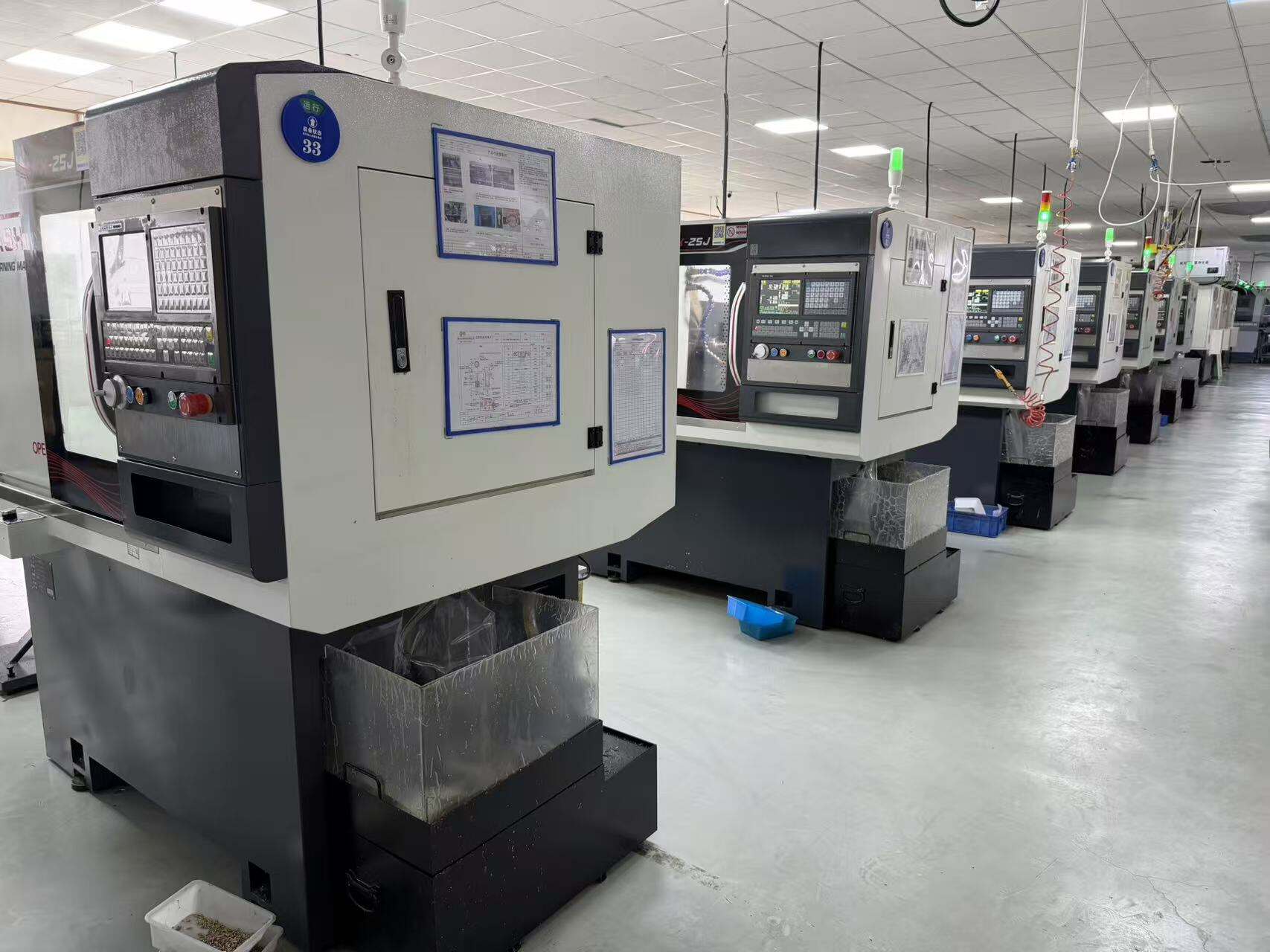
The labor economics of custom metal stamping provide substantial advantages over alternative manufacturing methods. Once properly set up, custom metal stamping operations require minimal direct labor intervention, with automated feeding systems and progressive dies enabling continuous production with limited operator oversight. This contrasts sharply with machining operations that may require constant monitoring, tool changes, and manual part handling. The reduction in direct labor requirements translates to lower per-part labor costs, especially significant in high-volume electronics production where labor expenses can compound quickly.
Custom metal stamping also reduces the skill level requirements for production operators compared to complex machining operations. While tool and die setup requires specialized expertise, the actual stamping operation can be managed by operators with basic training, reducing both wage costs and training investments. The consistency of custom metal stamping processes also minimizes the potential for human error, reducing rework costs and quality-related labor expenses that can accumulate in more manual manufacturing processes.
Speed and Volume Production Benefits
High-Speed Manufacturing Capabilities
The speed capabilities of custom metal stamping directly correlate to cost-effectiveness in electronics manufacturing. Modern stamping presses can operate at rates exceeding 1,000 strokes per minute, with progressive dies capable of producing complete parts in a single press stroke. This production speed advantage becomes particularly pronounced when compared to machining operations that may require multiple setups and tool changes to achieve similar geometries. The time savings translate directly to reduced manufacturing costs per unit, making custom metal stamping especially attractive for high-volume electronics components.
Progressive die custom metal stamping can perform multiple operations simultaneously, including cutting, forming, piercing, and finishing operations in a single pass through the press. This eliminates the need for multiple machine setups and part transfers between operations, further reducing cycle times and associated costs. For electronics manufacturers dealing with tight production schedules and just-in-time delivery requirements, the speed advantages of custom metal stamping provide both cost benefits and operational flexibility that support responsive manufacturing strategies.
Scalability and Volume Economics
Custom metal stamping demonstrates exceptional scalability characteristics that align perfectly with electronics industry volume requirements. While initial tooling investment may appear substantial, the cost per part decreases dramatically as production volumes increase. This scalability makes custom metal stamping particularly cost-effective for electronics applications where component volumes may range from thousands to millions of units annually. The ability to maintain consistent quality and dimensional accuracy across these volume ranges ensures that cost benefits don't come at the expense of product reliability.
The volume economics of custom metal stamping become even more favorable when considering the tooling longevity typical in well-designed stamping operations. Quality stamping dies can produce millions of parts before requiring significant maintenance or replacement, amortizing the initial tooling investment across substantial production volumes. For electronics manufacturers planning multi-year product lifecycles, this tooling durability provides predictable cost structures that support accurate financial planning and pricing strategies.
Quality Consistency and Reduced Secondary Operations
Dimensional Accuracy and Repeatability
The dimensional consistency achieved through custom metal stamping eliminates many secondary operations that would otherwise be required to achieve electronics industry specifications. Modern stamping dies can maintain tolerances within ±0.001 inches across millions of production cycles, ensuring that each part meets exact specifications without additional machining or finishing operations. This consistency reduces both direct processing costs and quality control expenses associated with dimensional verification and sorting operations.
The repeatability of custom metal stamping processes also minimizes the variation that can lead to assembly problems or field failures in electronics applications. When components consistently meet specifications, downstream assembly operations experience fewer disruptions, reducing labor costs and improving overall production efficiency. The elimination of sorting or selective assembly processes that might be required with less consistent manufacturing methods provides additional cost benefits that accumulate across high-volume production runs.
Surface Finish and Functional Features
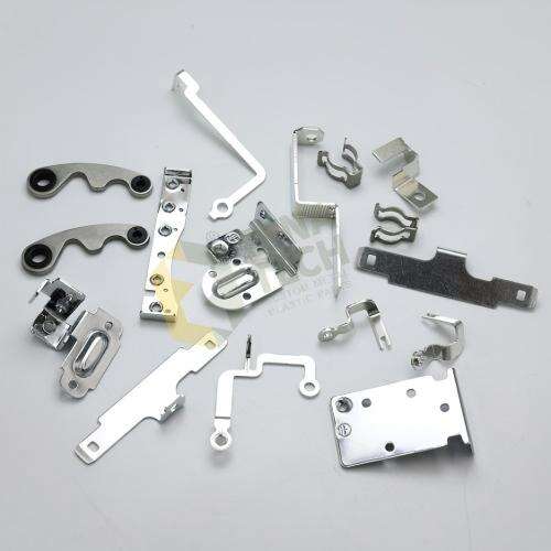
Custom metal stamping can incorporate surface finishing and functional features directly into the stamping process, eliminating secondary operations that would otherwise add cost and complexity. Coining operations can create precise surface textures, while forming operations can establish functional features like springs, clips, or mounting tabs without additional manufacturing steps. For electronics components that require specific surface conditions for electrical conductivity or assembly purposes, integrated finishing capabilities provide both cost savings and improved functionality.
The ability to create complex three-dimensional geometries in custom metal stamping operations reduces the need for welding, brazing, or mechanical assembly of multiple components. Single-piece construction eliminates joint failure modes while reducing material costs and assembly labor. For electronics applications where reliability and cost control are both critical, this integration of multiple functions into single stamped components provides compelling economic advantages while maintaining or improving product performance.
Tooling Investment and Long-Term Cost Analysis
Initial Investment Justification
While custom metal stamping requires upfront tooling investment, the long-term cost analysis clearly demonstrates superior economics for electronics manufacturing applications. The initial die cost must be evaluated against the total lifecycle cost of component production, including material costs, labor expenses, quality costs, and overhead allocation. When analyzed across typical electronics production volumes, custom metal stamping tooling investments typically achieve payback within the first year of production, with subsequent years providing substantial cost advantages over alternative manufacturing methods.
The tooling investment in custom metal stamping also provides manufacturing flexibility that supports product evolution and design optimization. Progressive dies can often be modified to accommodate design changes or improvements without complete retooling, allowing electronics manufacturers to respond to market demands while preserving their tooling investment. This adaptability provides additional economic value that extends the useful life of stamping tooling beyond initial product designs.
Total Cost of Ownership Considerations
Custom metal stamping delivers superior total cost of ownership when all factors affecting electronics component costs are considered comprehensively. Beyond direct manufacturing costs, custom metal stamping provides advantages in inventory management, quality control, and supply chain complexity that contribute to overall cost-effectiveness. The high production rates possible with custom metal stamping reduce work-in-process inventory requirements while the consistency of the process minimizes safety stock needs for quality-related issues.
The predictable nature of custom metal stamping operations also supports lean manufacturing initiatives that further reduce total ownership costs. Consistent cycle times enable accurate production planning and scheduling, reducing expediting costs and improving customer service levels. The reduced complexity of custom metal stamping compared to multi-operation machining processes simplifies production control and reduces the administrative overhead associated with complex manufacturing routing and scheduling requirements.
FAQ
What volume thresholds make custom metal stamping most cost-effective for electronics components?
Custom metal stamping typically becomes cost-effective for electronics components at volumes exceeding 10,000 units annually, with optimal economics achieved above 50,000 units per year. The exact threshold depends on part complexity, material costs, and alternative manufacturing options, but the fixed tooling costs are generally justified when amortized across these volume levels. For highly complex parts or those using expensive materials, lower volume thresholds may still justify custom metal stamping investment.
How does custom metal stamping compare to other manufacturing methods for electronics cost control?
Custom metal stamping generally provides 30-50% cost savings compared to machining for high-volume electronics components, with additional advantages in cycle time and material utilization. Compared to fabrication methods like laser cutting followed by forming, custom metal stamping offers 20-40% cost advantages while providing superior dimensional consistency. The cost benefits increase with production volume and part complexity, making custom metal stamping particularly attractive for electronics applications requiring both cost control and quality consistency.
What factors should electronics manufacturers consider when evaluating custom metal stamping economics?
Electronics manufacturers should evaluate total lifecycle costs including tooling amortization, material utilization, labor requirements, quality costs, and inventory implications when assessing custom metal stamping economics. Production volume projections, part complexity, tolerance requirements, and material specifications all influence the economic analysis. Additionally, considerations of supply chain flexibility, delivery requirements, and future design change potential should be factored into the evaluation to ensure optimal manufacturing strategy selection.
How does material choice affect the cost-effectiveness of custom metal stamping in electronics?
Material selection significantly impacts custom metal stamping cost-effectiveness, with the high material utilization rates of stamping providing greater advantages for expensive materials like specialized alloys or precious metals common in electronics. Softer materials like copper and aluminum stamp more easily, reducing tool wear and extending die life, which improves long-term economics. However, custom metal stamping remains cost-effective even for harder materials when production volumes justify the tooling investment and the material savings offset any increased tool maintenance costs.
Table of Contents
- Economic Advantages of Custom Metal Stamping in Electronics Production
- Speed and Volume Production Benefits
- Quality Consistency and Reduced Secondary Operations
- Tooling Investment and Long-Term Cost Analysis
-
FAQ
- What volume thresholds make custom metal stamping most cost-effective for electronics components?
- How does custom metal stamping compare to other manufacturing methods for electronics cost control?
- What factors should electronics manufacturers consider when evaluating custom metal stamping economics?
- How does material choice affect the cost-effectiveness of custom metal stamping in electronics?