Capacitates Fabricandi Ultra-Praecisionis
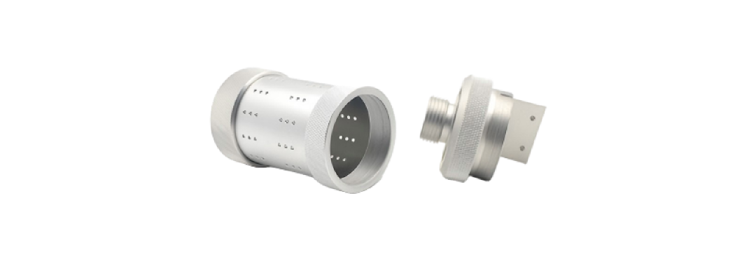
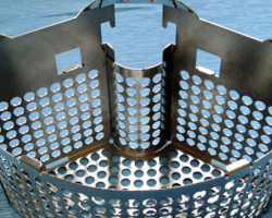
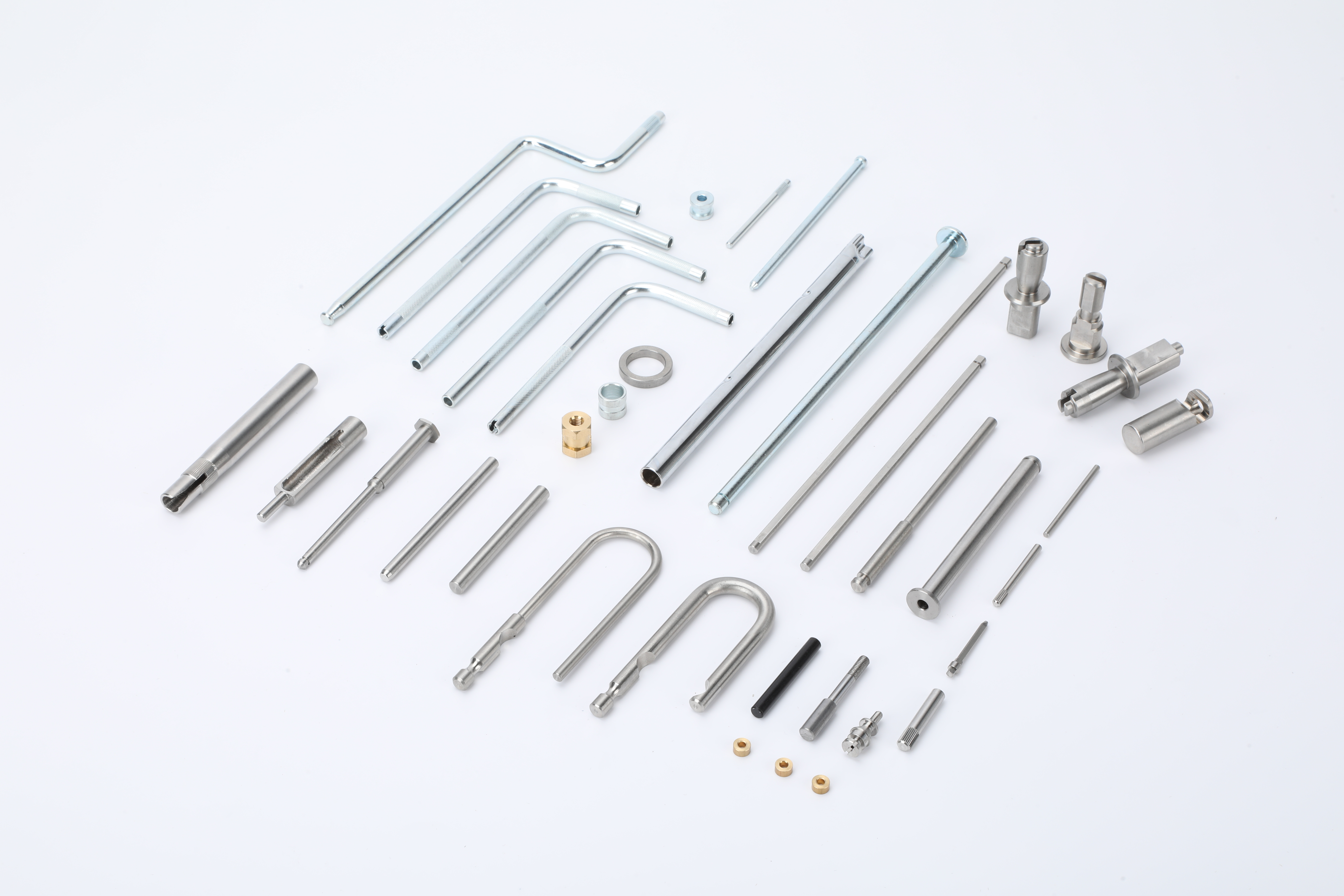
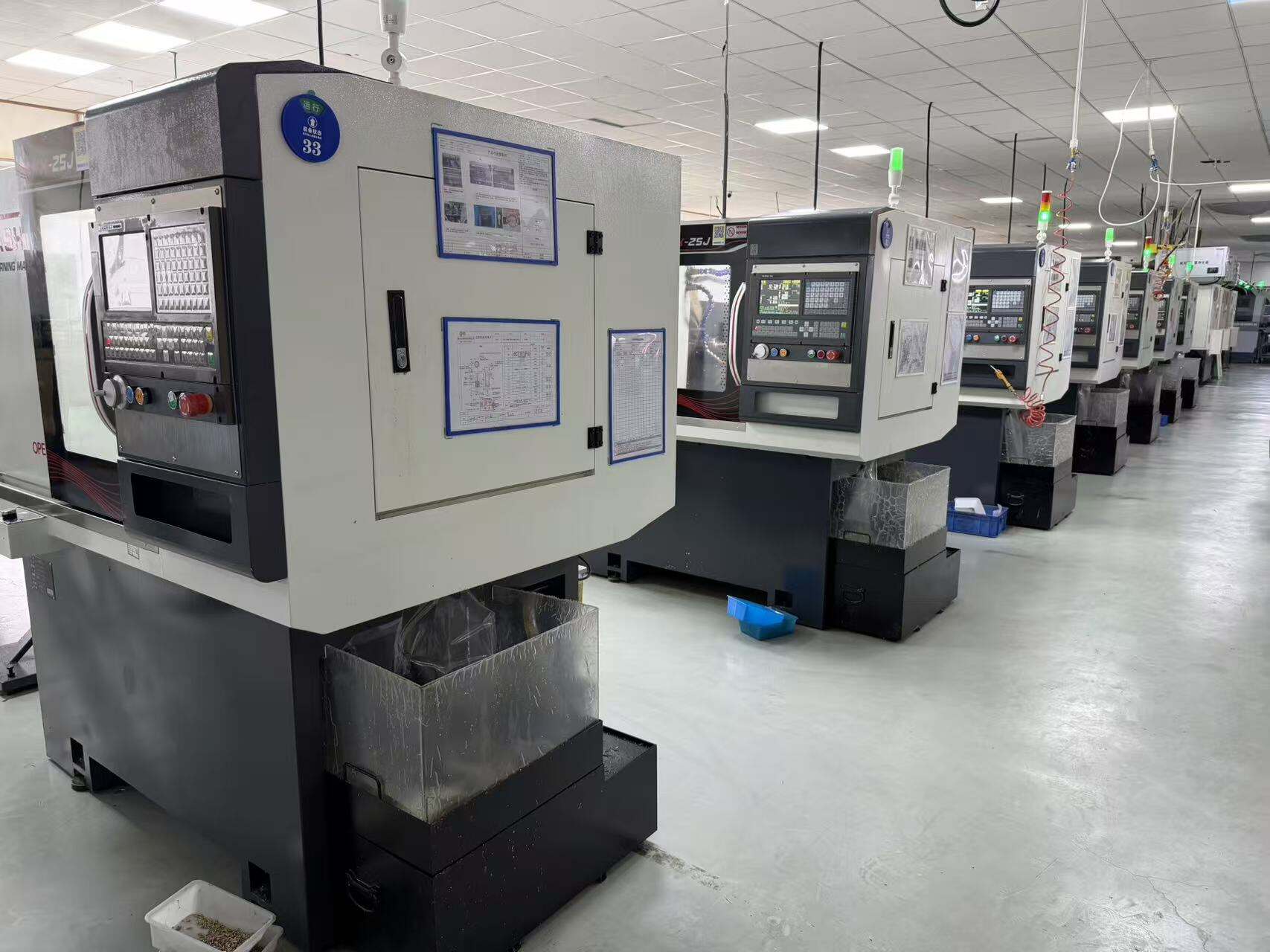
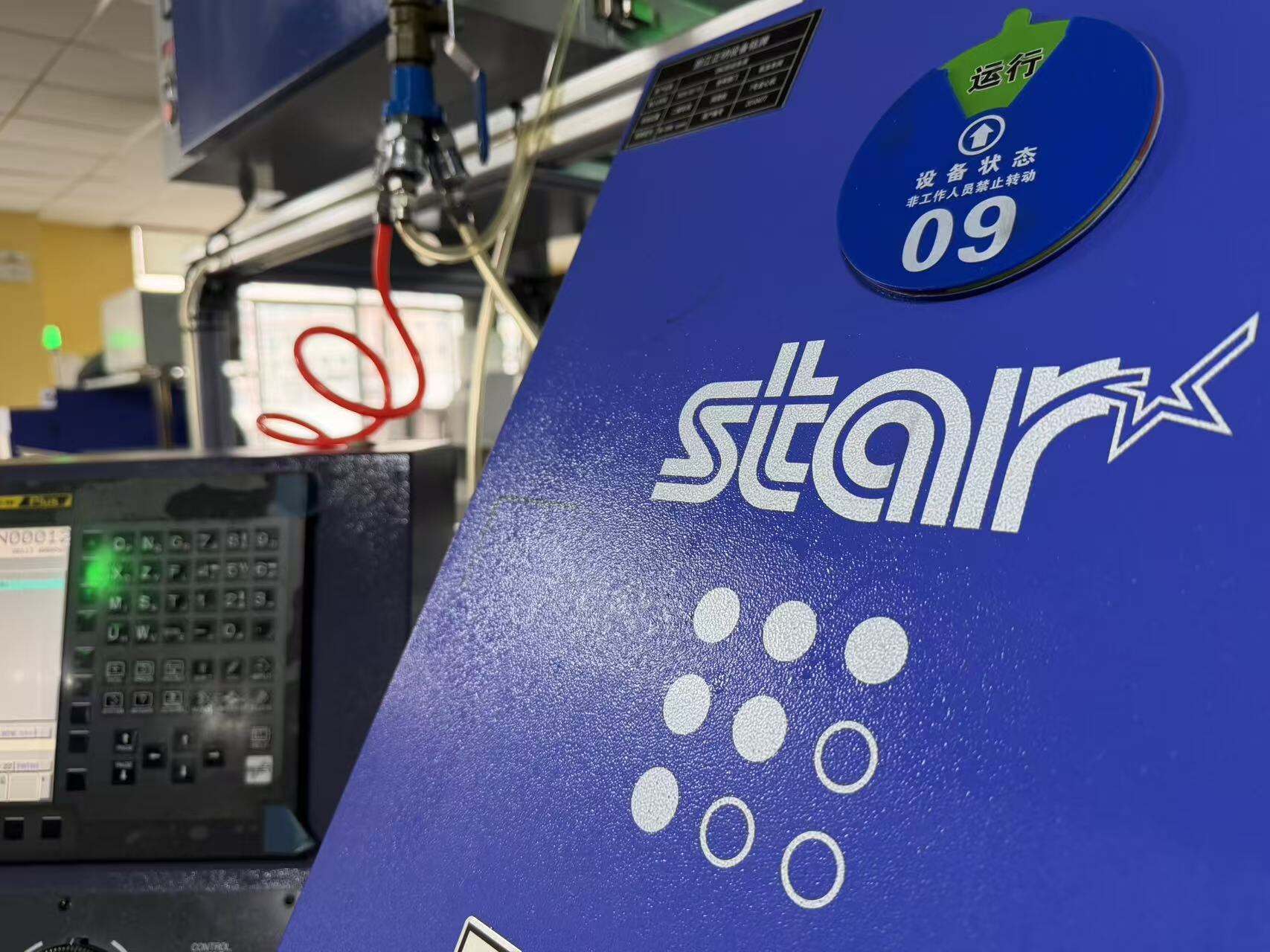
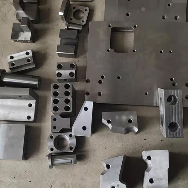
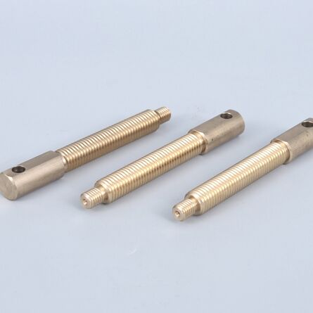
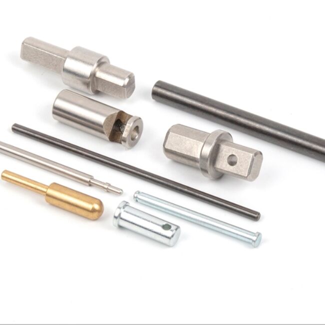
Machinatio praecisa semiconductorum per CNC adhibens semiconductores ad altissimum gradum praecisionis pervenit, qui normam auream pro fabricandis componentibus semiconductorum constituit. Haec technologia constanter tolerentias dimensionales intra 1–2 micrometra praebet, quae methodos machinationis consuetas magnopere superant. Hae facultates praecisionis ex systematibus motorum servo provectis oriuntur, quae accuratam positionem usque ad nanometra praebent, ut omnis componentis exactis specificatis, quae ad applicationes semiconductorum requiruntur, satisfaciat. Systemata controlis multi-axialia operationes machinationis simul in pluribus planis permittunt, geometrias complexas creando dum tamen tolerentiae angustae per totum componentem serventur. Algorithmi compensationis temperaturae expansionem thermicam automato corrigunt, ut accuratio etiam in productionibus diuturnis vel sub condicionibus ambientalibus variabilibus maneat. Integratio systematum mensurationis laseris verificatonem dimensionalem in tempore reali praebet, quae correctiones statim permittit, si quae deviatio in ipso processu machinationis detegitur. Qualitas superficiei ad gradum egregium pervenit, cum valores asperitatis infra 0,05 micrometra attingi possint, quod ad componentes semiconductorum, qui superficies speculares pro optima functione postulant, necessarium est. Haec praecisio etiam ad micro-structuras, ut foramina parva, scissurae, et paterna intricata, quae in instrumentis et fixationibus semiconductorum vulgo inveniuntur, extenditur. Factor repetibilitatis certum facit ut milia componentium identicorum produci possint sine fere ulla variatione, quod ad fabricationem semiconductorum in magnis quantitatibus necessarium est, ubi constantia directe in rationem reditus dispositivorum incidit. Technologia provecta axis rotantis velocitatem rotandi constantem servat et eccentricitatem minuit, quod ad superficies optimas et accuratam dimensionem confert. Systemata isolationis vibrationum perturbationes externas tollunt, quae praecisionem machinationis laedere possent, dum constructio rigida machinae stabilitatem praebet, quae ad consequendos resultatus constantes necessaria est. Protocolla asservationis qualitatis proceduras mensurationis comprehensivas includunt, quae omnem dimensionem criticam verificant antequam componentes e fabrica exeant.